Qualcomm's two new flagships share one spec sheet, and the memory clock that binds on-device AI has not moved
Qualcomm launched the Snapdragon 8 Elite Gen 6 and 8 Elite Extreme Gen 6 on 21 September 2026, both pitched on agentic on-device AI. Neither product brief states an NPU throughput figure, a memory bus width, or the largest model the platform can hold.
By Parminder Kumar Sharma · · 20 min read

The one number on the sheet that did not move
Qualcomm's Snapdragon 8 Elite Gen 5 product brief, document 87-93124-1 Rev B, states the platform's memory support in two lines: "Support for LP-DDR5x memory, up to 5300MHz" and "Memory Density: Up to 24GB". The Snapdragon 8 Elite Gen 6 product brief, document 87-A3018-1 Rev A, published on 21 September 2026, states "Support for LP-DDR5x/6, up to 5300 MHz" and "Memory Density: Up to 24GB". The Snapdragon 8 Elite Extreme Gen 6 brief, 87-A3019-1 Rev A, states exactly the same two lines.
The clock is the same. The capacity ceiling is the same. On the published record, across a full generation, the memory subsystem that feeds every one of the AI blocks Qualcomm spent this launch talking about carries the same headline number it carried last year.
That matters more than it looks, because generating text with a language model is not a compute problem on a phone. It is a memory problem. To produce each token, the processor has to read the model's active weights out of DRAM. Compute units sit idle waiting for those bytes. The ceiling on how fast a local assistant can answer is memory bandwidth divided by the weight bytes read per token, and nothing on the NPU can raise a ceiling set by the bus.
Qualcomm announced both parts on 21 September 2026 at Snapdragon Summit. The press release names nine launch partners, HONOR, iQOO, Motorola, OnePlus, OPPO, REDMI, RedMagic, vivo and Xiaomi, and contains no numbers at all: no clock, no capacity, no percentage, no throughput. Every quantified claim in this briefing comes from the two product pages and the three product briefs, which are the only documents on the record that carry figures.
The blocks Qualcomm names, and the number missing from all of them
A silicon launch is a list of named blocks, and the names are the story, because each one is a claim about what the part does and a boundary around what the vendor is willing to be held to. The Gen 6 brief names eight functional blocks plus memory. Here is what each of them is, stated only from the brief.
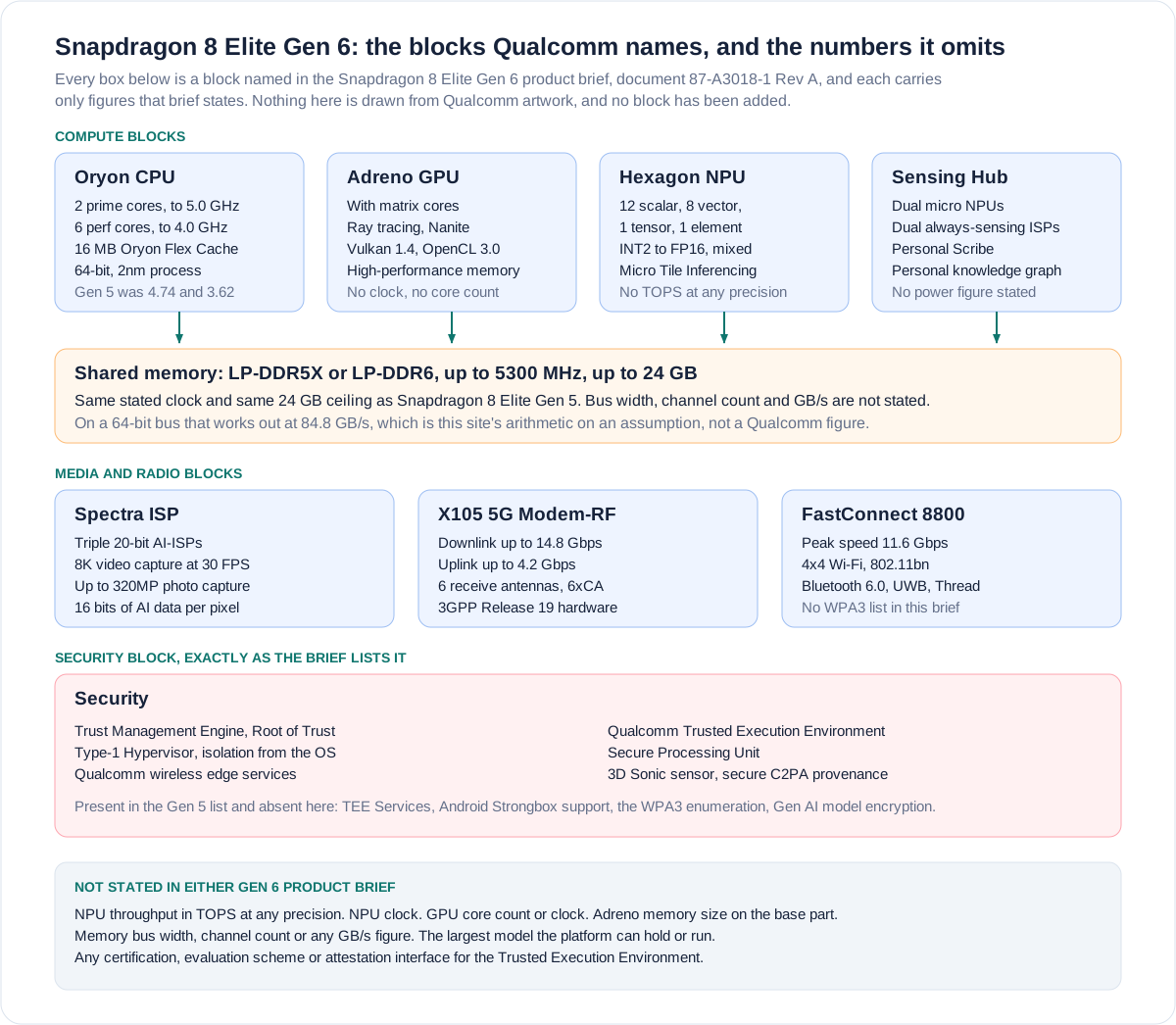
Every named block in the Snapdragon 8 Elite Gen 6 product brief, 87-A3018-1 Rev A, with what the brief states and what it leaves out
| Block | What the brief states | What the brief does not state |
|---|---|---|
| Oryon CPU | 2 prime cores to 5.0 GHz, 6 performance cores to 4.0 GHz, 16 MB Oryon Flex Cache, 64-bit, 2nm | Which Oryon generation the base part uses. The base page says "next generation", the Extreme page says 4th generation |
| Adreno GPU | Matrix cores, hardware ray tracing with Lumen, Nanite, Vulkan 1.4, OpenCL 3.0 | Any clock, any core count, and the size of Adreno high-performance memory on the base part |
| Hexagon NPU | 12 scalar, 8 vector, 1 tensor, 1 element; INT2 to FP16 with mixed precision; Micro Tile Inferencing; 64-bit memory virtualisation | Throughput in TOPS at any precision, the NPU clock, and the size of NPU shared memory |
| Sensing Hub | Dual micro NPUs for audio, voice and sensors; dual always-sensing ISPs for two concurrent always-sensing cameras; Personal Scribe | Power draw, what the personal knowledge graph retains, for how long, and where it is stored |
| Spectra ISP | Triple 20-bit AI-ISPs, 8K capture at 30 FPS, up to 320MP photo capture, 16 bits of AI data per pixel | Whether always-sensing capture is visible to the host operating system or to a management agent |
| X105 5G Modem-RF | 14.8 Gbps downlink, 4.2 Gbps uplink, 6 receive antennas, 6xCA at 500 MHz, 3GPP Release 19 hardware, NR-NTN and NB-NTN | Which satellite operators or networks the non-terrestrial modes actually work on, and when |
| FastConnect 8800 | 11.6 Gbps peak, 802.11bn, 4x4 Wi-Fi, Bluetooth 6.0 with channel sounding, UWB, Thread 1.4 | Any Wi-Fi security modes at all. The Gen 5 brief enumerated four WPA3 modes; the Gen 6 briefs enumerate none |
| Security | Trust Management Engine as Root of Trust, Qualcomm TEE, Type-1 Hypervisor, Secure Processing Unit, wireless edge services, 3D Sonic, secure C2PA | Any certification, evaluation scheme, assurance level or attestation interface for any of those six items |
| Memory | LP-DDR5X or LP-DDR6, up to 5300 MHz, up to 24 GB density | Bus width, channel count, or any bandwidth figure in gigabytes per second |
What the memory figure actually permits, with the arithmetic shown
Qualcomm does not publish a bandwidth figure, so here is the calculation and its assumption, stated plainly so it can be argued with.
The brief states 5300 MHz. LPDDR is double data rate, so the transfer rate is 5300 x 2, or 10,600 mega-transfers per second. Bandwidth is transfer rate multiplied by bus width. The bus width is the number Qualcomm does not give. Eight-series Snapdragon parts have conventionally used a 64-bit memory interface, so taking 64 bits, or 8 bytes, per transfer:
10,600 MT/s x 8 bytes = 84,800 MB/s, which is 84.8 GB/s.
That figure is inference, not reporting. If the interface is wider, or if an LPDDR6 configuration organises its channels differently, the real number is higher and Qualcomm has chosen not to say so.
Take the 84.8 GB/s and divide by the weight bytes a dense model must read per token. An 8 billion parameter model quantised to 4 bits holds 4 GB of weights, so 84.8 divided by 4 gives a ceiling of 21.2 tokens a second. The same model at 8 bits holds 8 GB and halves to 10.6. A 13 billion parameter model at 4 bits is 6.5 GB and gives 13.0. A 30 billion parameter dense model at 4 bits is 15 GB of weights and gives 5.7, which is slower than most people read.
These are ceilings, not benchmarks. Real throughput is lower, because attention state and activations compete for the same bus and no memory system runs at its theoretical peak. The shape of the curve is the point.
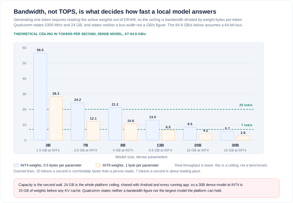
Capacity is the second wall, and it is the harder one. The 24 GB ceiling is the whole platform's memory, shared with Android, the launcher, the browser and every background app. Nothing like all of it is available for model weights. A 30 billion parameter dense model at 4 bits needs 15 GB resident before a single token of context is cached, which on a 24 GB handset is not a realistic steady state and on a 12 GB handset is impossible.
This is precisely where mixture-of-experts architectures earn their keep, because they decouple the two walls. A sparse model holds all its weights in memory but reads only the active experts per token, so it pays the capacity cost in full and only a fraction of the bandwidth cost. Launch coverage reports Qualcomm claiming the Extreme part's NPU can run mixture-of-experts models above 30 billion parameters. That claim appears in neither product brief and on neither product page. It rests on secondary reporting of a Qualcomm statement, and this briefing treats it as unverified.
Two parts, one spec sheet, and a difference nobody has quantified
Qualcomm's own framing is a "multi-flagship strategy" giving OEMs choice. The press release says the base part is "built on the same advanced 2nm process node" and powers "many of the same breakthrough AI, gaming, imaging, and connectivity features" as the Extreme.
Read the two specs and features sheets side by side and the word "many" is doing very little work. The CPU section is identical, character for character: two prime cores to 5.0 GHz, six performance cores to 4.0 GHz, 16 MB of Oryon Flex Cache, 64-bit. The memory section is identical. The display, audio, location, charging, modem and Wi-Fi sections are identical. The security section is identical. The part numbers differ, SM8950 against SM8975.
Where the two Gen 6 parts actually diverge on the record
Compiled line by line from the Snapdragon 8 Elite Gen 6 Product Brief (87-A3018-1 Rev A) and the Snapdragon 8 Elite Extreme Gen 6 Product Brief (87-A3019-1 Rev A)
| Item | 8 Elite Gen 6 | 8 Elite Extreme Gen 6 | Not stated for either |
|---|---|---|---|
| CPU | 2 prime to 5.0 GHz, 6 performance to 4.0 GHz, 16 MB Flex Cache | Identical, character for character | Why identical silicon yields 10 per cent on one part and 13 per cent on the other |
| Process and memory | 2nm; LP-DDR5X/6 to 5300 MHz; 24 GB; UFS 5.0 | Identical | Foundry, bus width, or any bandwidth figure |
| NPU | 12 scalar, 8 vector, 1 tensor, 1 element; Element Accelerator; INT2 to FP16 | Same, plus one extra line: 50 per cent larger shared memory | The size of that shared memory, before or after the 50 per cent |
| GPU | Adreno GPU with matrix cores; ray tracing; Nanite | Adreno Neural Fusion; matrix cores; MegaLights; 18 MB high-performance memory | Core count or clock for either part |
| Video decode | H.265, VP9, AV1 | Adds H.266 | Whether the base part can gain H.266 in software |
| Camera | 8K at 30 FPS; 4K slow motion at 120 FPS | 8K at 60 FPS; 4K slow motion at 240 FPS; APV capture | Which sensors and thermal envelopes those modes require |
| Security block | Seven lines | The same seven lines, word for word | Any difference at all between the two parts |
| Part number | SM8950 | SM8975 | Whether these are the same die at different bins |
So the honest answer to "what is different" is: the GPU, one NPU memory line, one video decoder, and the camera pipeline. Not clocks, not core counts, not cache, not memory support. Every published CPU and memory figure is shared.
Which makes the uplift claims hard to read. The base part claims 10 per cent better CPU performance against Gen 5 and the Extreme claims 13 per cent, against the same baseline, from a CPU section that is identical on both sheets. Qualcomm names no workload for either figure. There are perfectly ordinary explanations, sustained thermal headroom, memory controller tuning, a different bin, a different benchmark, and Qualcomm states none of them. A reader cannot tell from the record which one applies, and that is a fact about the record rather than about the silicon.
The security block is a list of names, not a level of assurance
Here is the whole of what Qualcomm claims about security on both Gen 6 parts, quoted in full because it is short: a Trust Management Engine described as a Root of Trust "with platform-level security foundations"; a Qualcomm Trusted Execution Environment; a Qualcomm Type-1 Hypervisor "for isolation from the high-level OS"; a Secure Processing Unit; Qualcomm wireless edge services; the 3D Sonic and 3D Sonic Max fingerprint sensors; "Secure C2PA AI provenance data support"; and "Enhanced AI processing isolation and model protection".
That is the complete list. It is identical on the base part and the Extreme.
Every item in it is a name for a place where code runs or a thing that exists. Not one is a statement about what has been evaluated, by whom, against what, or what an attacker would have to do to get past it. "Trusted Execution Environment" describes an architecture, not an assurance level. A TEE is a boundary; whether that boundary holds depends on the firmware inside it, the interfaces exposed to it, and the update path that keeps it patched, and none of those are in scope for a product brief. "Enhanced AI processing isolation" is enhanced relative to something the brief does not identify. "Secure C2PA AI provenance data support" is the only line that names an external standard and is therefore the only line a procurement team can test against a published specification.
This is not a criticism of the engineering, which may well be excellent. It is a statement about what the document does. A product brief is a sales artefact aimed at handset makers, not a security target, and it should be read as one.
What is more interesting is the comparison with last year's sheet, because four qualifications present in the Gen 5 brief are not in either Gen 6 brief.
Security and Wi-Fi lines quoted from the Snapdragon 8 Elite Gen 5 Product Brief (87-93124-1 Rev B) against the corresponding lines in both Gen 6 briefs
| Line | Snapdragon 8 Elite Gen 5 brief | Both Gen 6 briefs |
|---|---|---|
| Trusted Execution Environment | "Qualcomm Trusted Execution Environment (TEE) and Qualcomm TEE Services for use cases requiring higher processing assurance" | "Qualcomm Trusted Execution Environment (TEE)" |
| Secure Processing Unit | "Secure Processing Unit (SPU) with support for the Android latest Strongbox software components" | "Secure Processing Unit (SPU)" |
| Wireless edge services | "Qualcomm wireless edge services (WES) for secure attestation and provisioning" | "Qualcomm wireless edge services (WES)" |
| NPU model protection | "Support for Gen AI model encryption for extra security", listed under the NPU | No equivalent line under the NPU on either part |
| Wi-Fi security | "Wi-Fi Security: WPA3-Enterprise, WPA3-Enhanced Open, WPA3 Easy Connect, WPA3-Personal" | No Wi-Fi security line of any kind |
What on-device inference does to a BYOD or MDM policy
Strip the marketing away and the governance consequence of this launch is one sentence: the pitch is an assistant that reads your device, learns from your behaviour and acts across your apps, and does it all without the data leaving the handset.
Qualcomm says this in its own words. The base product page describes "personalized on-device agents that anticipate and act on your behalf" with "on-device learning adapting to your preferences over time keeping your data safe and secure". The base brief describes the Sensing Hub, the Hexagon NPU and the Oryon CPU working together so the platform can "understand your intent, access your personal context, map out a plan, and coordinate tasks across apps". The Extreme page promises "a persistent understanding of your world".
For a security team that is a genuinely new shape of problem, and the usual controls do not address it. Nearly every mobile control in common use is built around the assumption that something interesting leaves the device: a proxy sees the request, a cloud access broker sees the application, a data loss prevention rule sees the payload, a SIEM records the event. Local inference breaks all four at once. If the model runs on the NPU, there is no request, no payload and no event. The prompt containing a customer name, a contract clause or an unannounced financial figure is composed, processed and answered inside a package you cannot instrument and your MDM cannot see.
This is not a reason to panic, and it is arguably better for privacy than sending the same text to a cloud endpoint. But it is the end of egress as the place where mobile data governance happens, and no equivalent control has replaced it.
Three specific consequences follow from the spec sheet rather than from speculation.
Always-sensing is a design feature, not an edge case. Both briefs state that the Sensing Hub carries "Dual Always-Sensing ISPs to support two concurrent always-sensing cameras" and dual micro NPUs "for creating personal knowledge graphs". A persistent behavioural corpus built on the handset is the explicit product. Where that corpus lives on a dual-persona device, whether inside the Android work profile or outside it, is not stated in any of these documents, and it is an OEM and operating system question rather than a silicon one.
On-device learning breaks reproducibility. The Extreme page promises "on-device AI learning", and the base brief says the model adapts to "how you edit photos, write messages, and personalize visual experiences". If the model on the device changes with use, two handsets on the same corporate build will not behave the same way, and a behaviour you observed in testing may not be the behaviour in the field. Any assurance argument that relies on a fixed, testable configuration needs rewriting.
Provenance is the one control that produces readable evidence. "Secure C2PA AI provenance data support" is listed on both parts. C2PA is a published standard with verifiable signed manifests, which means media captured or edited on these devices can in principle carry an attestable record of how it was made. For anyone whose exposure is synthetic media rather than data leakage, that line is the most useful sentence in the whole brief.
What to do, in the order worth doing it
Take this with you
For anyone specifying 2027 handsets or writing a BYOD policy this quarter
- Write the missing numbers into the device tender rather than the chip review. Ask each OEM, in writing, for memory bus width and peak bandwidth in gigabytes per second, the largest model the device ships able to run locally, and the NPU throughput at a named precision.
- Ask every uplift claim the same two questions before it reaches a business case: measured against what baseline, and on what workload. The Gen 6 figures name the baseline, Snapdragon 8 Elite Gen 5, and name no workload at all.
- Ask the OEM to confirm in writing that the platform still backs Android StrongBox and still supports WPA3-Enterprise, because the Gen 6 product briefs no longer say so and the Gen 5 brief did.
- Decide now where the on-device personal knowledge graph is allowed to live on a dual-persona device, and make work profile containment a tender requirement rather than a discovery in year two.
- Accept that egress monitoring will not see locally processed prompts, and move the control to the point of data access instead: which corporate apps and which corporate data the on-device assistant may read.
- Stop treating a device baseline as fixed. If the vendor ships on-device learning, write reassessment into the assurance cycle rather than testing once at rollout.
- Ask for the silicon security update commitment in years, tied to the platform rather than the Android version, and make it a scored criterion.
- Use the C2PA provenance support. If your exposure includes synthetic media, require that capture provenance is enabled and that your verification tooling can read it.
The question that exposes the gap
Qualcomm has built a launch around agentic AI running locally, on a platform whose published memory clock and memory ceiling are identical to last year's, with no throughput figure for the processor doing the work and no bandwidth figure for the bus that feeds it. The two parts share a CPU section, a memory section and a security section, and differ by 3 percentage points on a CPU claim neither sheet explains.
None of that means the silicon is not faster. It very probably is. It means the published record cannot tell you by how much, on what, or within what limits, and a buyer committing a fleet to on-device AI is being asked to take the direction of travel on trust.
So the question to put to the handset maker, and to put in writing:
If the answer to the last part is "nothing", that is the honest state of mobile data governance in 2026, and it is worth knowing before the fleet arrives rather than after.
Key facts
Sources
- PrimarySnapdragon 8 Elite Gen 6 Mobile Platform product page: the source of the 10 per cent CPU, 35 per cent GPU, 14 per cent NPU and 20 per cent performance-per-watt claims, the specs spotlight and the Adreno high-performance memory figureQualcommaccessed 2026-09-23
- PrimarySnapdragon 8 Elite Extreme Gen 6 Mobile Platform product page: the source of the 13 per cent CPU, 44 per cent GPU, 35 per cent NPU, 33 per cent performance-per-watt and 85 per cent Sensing Hub claimsQualcommaccessed 2026-09-23
- PrimarySnapdragon 8 Elite Gen 6 Product Brief, document 87-A3018-1 Rev A: the full specs and features sheet used for every block, clock, cache, memory and security line in this pieceQualcommaccessed 2026-09-23
- PrimarySnapdragon 8 Elite Extreme Gen 6 Product Brief, document 87-A3019-1 Rev A: the full specs and features sheet used for the SKU comparisonQualcommaccessed 2026-09-23
- PrimarySnapdragon 8 Elite Gen 5 Product Brief, document 87-93124-1 Rev B: the baseline every Gen 6 percentage is measured against, and the source of the dropped security and Wi-Fi linesQualcommaccessed 2026-09-23
- PrimarySnapdragon 8 Elite Gen 5 product page: the previous generation's own uplift claims and the 4.74 GHz figureQualcommaccessed 2026-09-23
- PrimaryLaunch press release, 21 September 2026: the multi-flagship strategy, the OEM list, the same 2nm node statement, and the complete absence of numbersQualcommaccessed 2026-09-23
- Reported byLaunch coverage, used only for the claim that the NPU can run mixture-of-experts models above 30 billion parameters, which appears in neither product briefXDA Developersaccessed 2026-09-23